
Work:
Improving semiconductor power electronic material will have an affect felt throughout the power conversion industry mainly with improvements to breakdown field strength, conduction loss, and reliability. As part of a project with ARPA-E we were growing and fabricating PN diodes on Bulk GaN wafers which were commercially bought. Typically, MOCVD grown GaN is done on sapphire wafers but due to lattice mismatch and electrical conductivity problems, new work has begun trying to make growth on bulk GaN more attractive. My part in all of this is working with the material scientists in the group to create viable PN diode structures, taking the grown layers into a cleanroom environment to fabricate surface passivated and field-plated PN diodes, testing them in a probe station and finally analyzing the data.
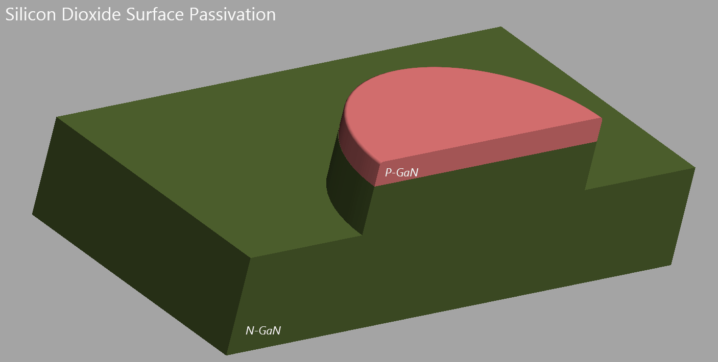
The figure above is being used just to show the parts of the final device that would be hard to understand in a static image, it does not show the actual fabrication process. When putting the diode into forward bias you inject minority carriers into the respective regions (holes into n-type, electrons into p-type) which creates a situation where radiative recombination can occur. Depending on the transition that is made, different light will come out. The figure below shows this very phenomena however, in GaN if the transition is happening from the valence to conduction band it wouldn’t be visible (363nm - UV). This implies that the transition may be occuring at trap levels in the forbidden gap likely there due to impurities. Additionally, if you watch long enough you’ll see little arc’s from the high electric field in reverse bias.