Problem:
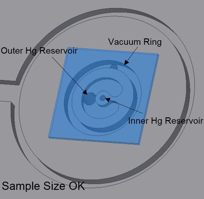
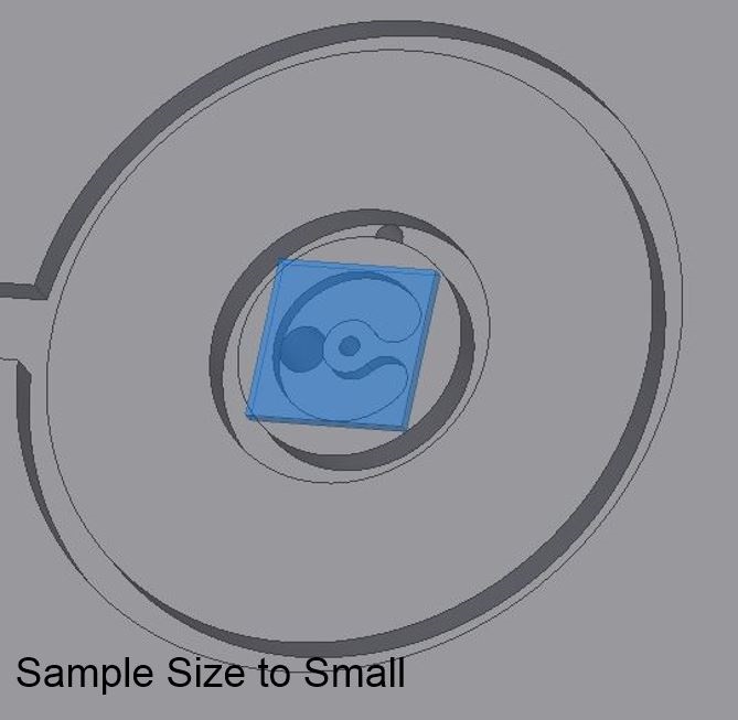
Being able to quickly and cheaply identify the free carrier concentration in a semiconductor layer can be helpful when slight changes to material growth parameters can increase or decrease contamination concentrations such as carbon. In GaN carbon has been shown to incorporate electrically as a deep-level trap near the mid-gap and decrease the overall carrier concentration. Thus when varying the carbon incorporation it would be good to know when your dopant atoms are compensated by contamination. A mercury probe system allows researchers to instantly make metal contacts on the top surface of a sample and run tests, such as measuring the free carrier concentration. However, the samples must be >1cm² to adequately cover a vacuum ring which pulls the mercury up onto the sample. We had a needed to measure small (<0.9cm²) samples and thus had to create an adapter.
Solution:
In order to measure these samples we only needed to keep pressure on the back while also sealing the sample so the vacuum could pull the mercury up onto the sample. This could have been done by laying a piece of flimsy rubber or tape on the back of the sample however, we also wanted to ability to make electrical contact to the back of the sample.
Hg Probe With Sample


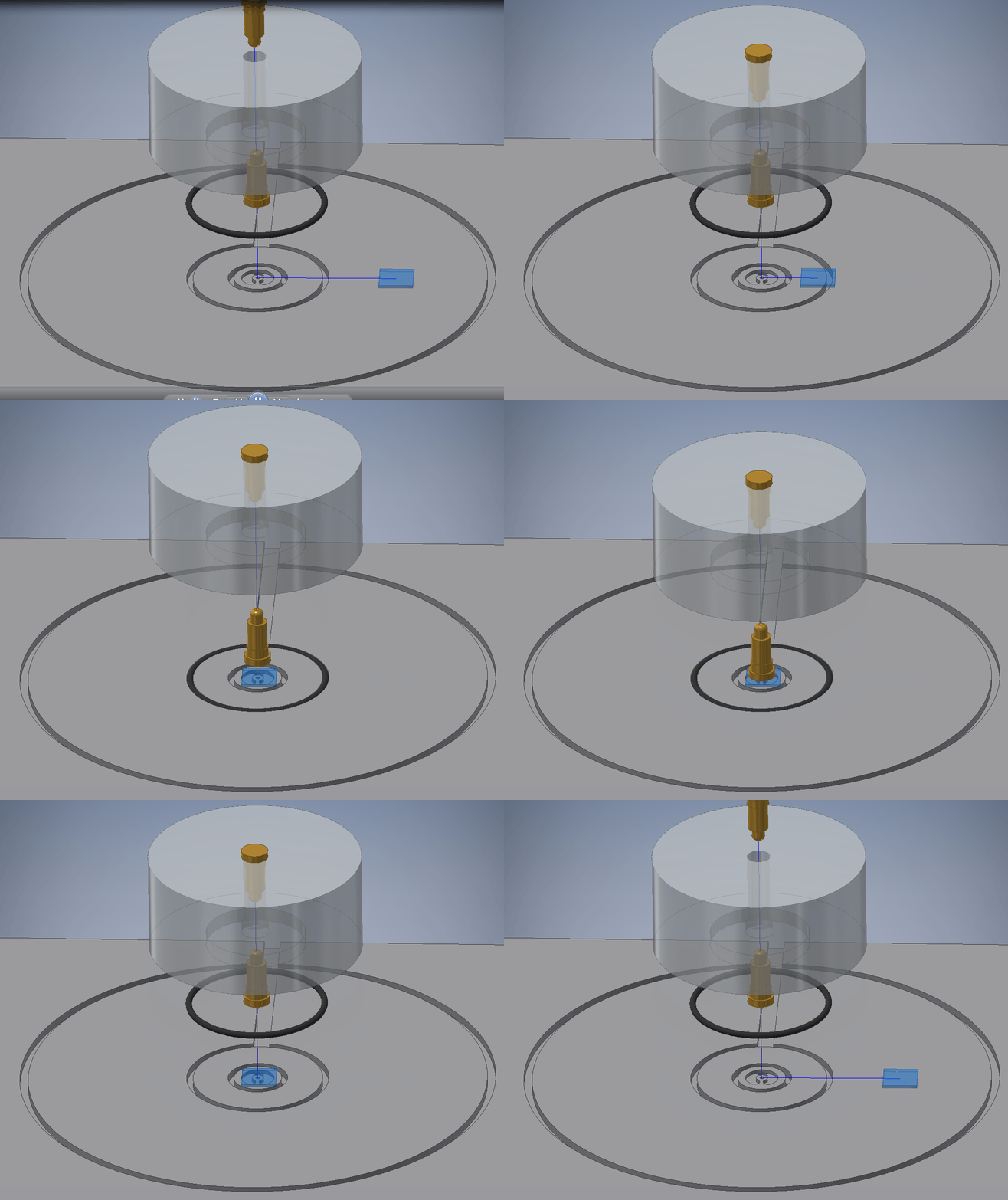
It was decided that because the Hg probe is made of acrylic that we could machine the adapter from the same material. We started with a 1.25” round, planarized the end, machined a recess for the sample to sit in, then dropped in two pogo pins, and finally glued the top pin to the adapter. The final product is shown below. The purpose of the pogo pins was to keep pressure on the sample while also making electrical contact to the back of it. Additionally, planarizing it helped seal the acrylic-acrylic interface so vacuum could be pulled in the sample recess.
Hg Probe With Adapter

Shown above is the 3D model assembly of the Hg probe adapter where you can see the sample (blue), an o-ring (black), the two pogo-pins (gold) and the machined acrylic adapter (grey).
